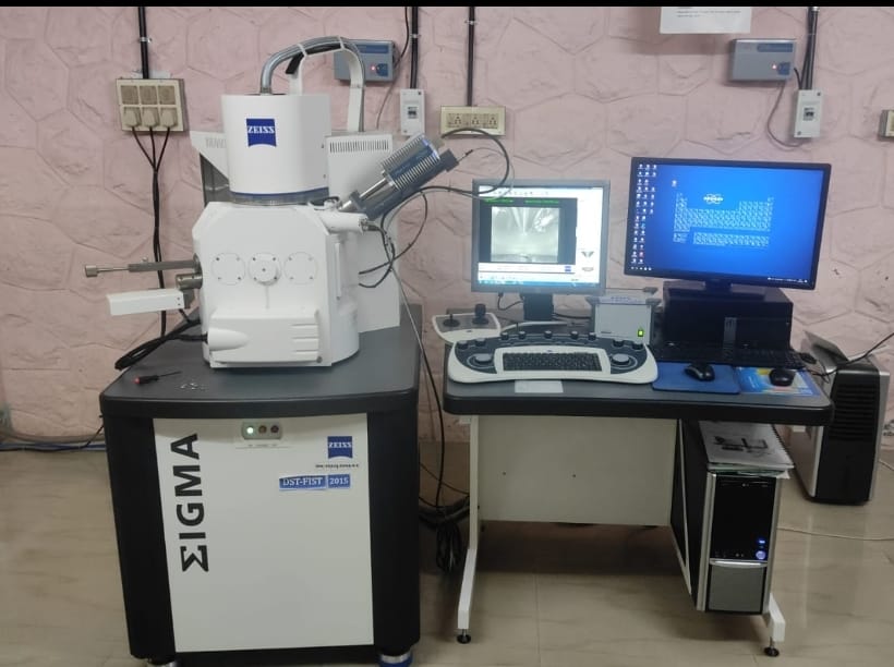
Field-Emission Scanning Electron Microscope (FE-SEM), Zeiss Sigma, provides excellent imaging properties combined with analytical capabilities makes this high end FE-SEM suitable for a wide range of applications in materials science, life science and semiconductor technology. The large specimen chamber for the integration of optional detectors and accessories enables the user to configure the Sigmafor specific applications without sacrificing productivity or efficiency. EDS (Energy X-Ray Dispersive Spectrometer (Bruker)) with Quantax X-flash ® 6 | 100 is also attached for chemical analysis and elemental mapping.
• GEMINI Technology with high efficiency in-lens detector and no magnetic field at  specimen level
• Superb resolution and image quality at high and low operating voltages
• Magnification ranges from 75x to 1000,000x
• Extremely wide operating voltage range from 0.2-30kV
• Designed-in ease of use with minimal adjustments required when changing operating  conditions
• Multi-User friendly with Windows® based SmartSEM control software and ESPRIT  software.
| Equipment | Model | Software |
|---|---|---|
| FESEM | Carl Zeiss Sigma | SMARTSEM |
| EDS | Bruker Quantax X-flash ® 6 | 100 | ESPRIT |
How to prepare samples for FESEM/EDS analysis ?
Because FESEM utilizes vacuum conditions and uses electron beam to form an image, special sample preparations is needed as listed below:
• The sample is mounted on carbon tape that is put on the surface of the stub.
• Approximate size of the sample 1 x 1 cm (max).
• All water must be removed from the samples because the water would vaporize in the vacuum.
• Electrically conductive samples do not require any preparation before being used, however the  samples must be completely dry and free from volatile substances.
• Non-conductive samples need to be made conductive by coating the sample (using sputter coater)  with a thin layer of conductive material like Au/Ag/C.